Ceramic PCBs
With the increasing popularity and availability of ceramic PCBs circuit designers have considerably more options at their disposal. Ceramic substrates have excellent thermal performance, Thermal Conductivity to 180W/mK, and can sustain high working temperatures. They are essential for high-power packages with thermal issues to solve.
Because of the mechanical and thermal advantages, ceramics have been utilised extensively in electronics and electronic components for many years. Recent technological and manufacturing advancements have led to the replacement of complete PCBs.
The main advantage ceramic has over more traditional materials like FR4 and Metal Clad PCBs is heat dissipation. The transfer of heat through the boards is much more effective when components are placed directly on the boards without the use of a dielectric layer.
Additionally, ceramic material has a very low CTE (Coefficient of Thermal Expansion), which gives circuit designers more compatibility options. Ceramic material can endure high operating temperatures (up to 800°C).
See a full list of advantages below:
GSPK specialises in Alumina Oxide (Al2O3), Aluminium Nitride (AIN), and Silicon Nitride (SiN) boards. Direct bond copper (DBC), direct plated copper (DPC) Active Metal Brazing (AMB), and Thick Film technologies are used for the circuitry depending on the requirements and/or applications.
Depending on the technology required or the end application, circuits can be printed using either Copper (Cu) or Silver (Ag).
If using a Copper (Cu) track, solder resist/ident/surface finish options are much the same as conventional PCBs. If Silver (Ag) is being used we use a clear/glass solder mask. Gold plating can also be used in certain applications where the silver pads require protection.
See below for more information on Al2O3, AIN, and other technologies available.
About
Alumina Oxide 96% is the most popular Ceramic substrate for PCBs. By the nature of the material it has excellent electrical insulation and exhibits excellent thermal characteristics. Although Alumina’s thermal conductivity is not as high as Aluminium Nitrides', it is still significantly greater than the best Metal Clad PCB materials, which have a thermal conductivity of about 24 W/mK for the 96% variant.
Alumina Oxide is a material that works well for LED applications because of its strong light reflection and favourable thermal characteristics. While having low thermal expansion and signal loss values, it can be used for a variety of applications, such as cooling systems, high-frequency systems, and sensor modules.
Advantages
Technical Specifications
Download our complete design rules and manufacturing capabilities below.
If you have different requirements, or have any questions please contact us.
About
Aluminium Nitride (AlN) is an ideal choice when a high thermal conductivity is needed. AlN has a better thermal conductivity than other materials; up to 180 W/mK.
AlN is suited for a wide range of applications, such as high power LEDs, testing, sensors, integrated components (ICs), and more. It also has a very low CTE and high operating temperatures .
Advantages
Technical Specifications
Download our complete design rules and manufacturing capabilities below.
If you have different requirements, or have any questions please contact us.
| Property | Unit | SiN |
|---|---|---|
| Thermal Conductivity | W/mK | 85 |
| Maximum Operating Temperature (MOT) | °C | 1000 |
| Coefficient of Thermal Expansion (CTE) | x 10¯6/K | 2.6 |
| Dielectric Constant | - | 9 |
| Signal Loss | x 10¯3 | 0.2 |
| Light Reflectivity | % | - |
| Breakdown Voltage | KV/mm | 15 |
| Rupture Strength | Mpa | 800 |
Active Metal Brazing (AMB) - Ceramic PCBs
Active Metal Brazing is a new novel technique for producing ceramics without metallization (AMB).
AMB "brazes" the copper directly to the ceramic substrate while operating at high temperatures in a vacuum.
AMB creates a substrate with exceptional heat dissipation qualities in a highly reliable substrate.
The brazing process is perfect for Power Electronics applications because it can create copper weights of up to 800µm on extremely thin ceramic substrates.
AMB Single Sided
The possible copper weights and matching substrate thicknesses are listed in the table below. It is always advised that the copper thickness be kept to no more than half the thickness of the ceramic for mechanical stability.
AMB Double Sided
With copper both sides a higher stability and mechanical strength is achieved enabling Heavy Copper to be offered on thin ceramic substrates. The following is a guide on double sided material availability although during the etching process original copper weights can be reduced.
| Active Metal Brazing Double Sided Panels | ||||||
|---|---|---|---|---|---|---|
| 200µm | 250µm | 300µm | 400µm | 500µm | 800µm | |
| 0.25mm | SiN AlN |
SiN AlN |
SiN | SiN | SiN | SiN |
| 0.32mm | SiN | SiN | SiN | SiN | SiN | SiN |
| 0.38mm | AlN | AlN | AlN | |||
| 0.63mm | AlN | AlN | AlN | AlN | AlN | |
| 1.00mm | AlN | AlN | AlN | AlN | AlN | AlN |
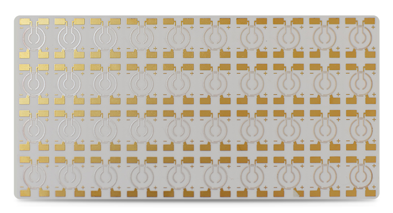
 Immersion Tin Panel
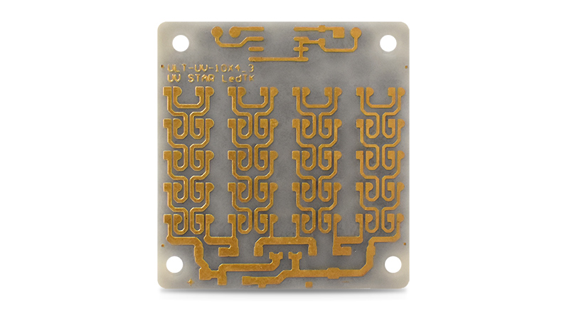 AIN used for UV LED products
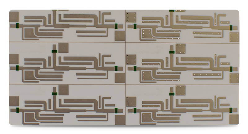
 Silver Paste Conductor with ENIG surface treatment
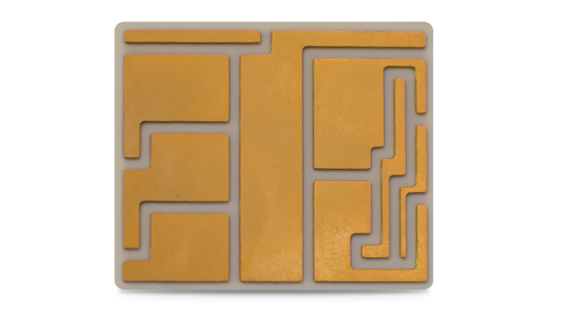 Direct Bond Copper
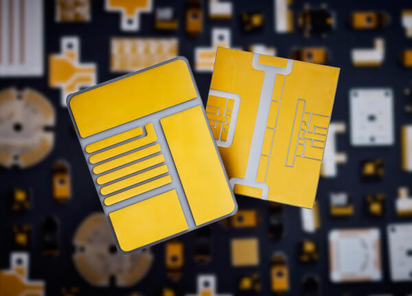
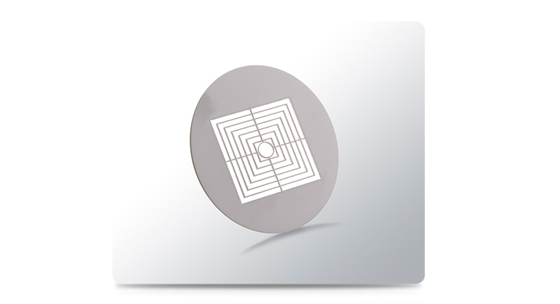 Alumina Oxide Al203
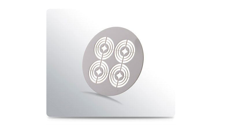 Alumina Oxide Al203
GSPK Circuits Ltd
Wetherby Road, Boroughbridge
North Yorkshire
YO51 9UY
United Kingdom
+44 (0)1423 798 740
enquiries@gspkcircuits.ltd.uk


GSPK Circuits Ltd. is a market leading UK PCB manufacturer & global supplier of Printed Circuit Boards. We focus on Fast-turn PCBs, Prototyping and Specialist PCBs. Our team manages your PCBs and ensures you get a product with the highest quality. Having the 'Lean Champion' status, you're ensured a fast and agile approach to PCB manufacture in one of our world class manufacturing divisions.