
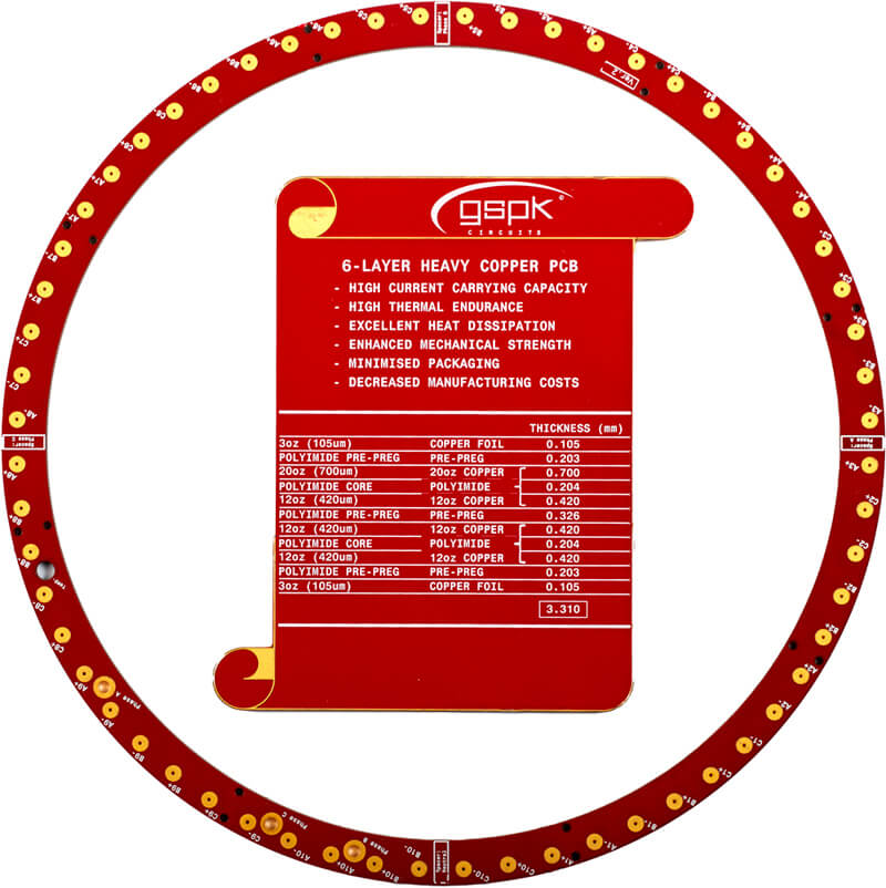
Printed Circuit Boards For High Power
Engineers and designers working with power electronics are benefiting from the growing trend for Heavy and Extreme Heavy Copper PCBs.
Heavy Copper: 5 oz, 175µm, 0.175mm and above
Extreme Heavy Copper: 15 oz, 525µm, 0.525mm and above
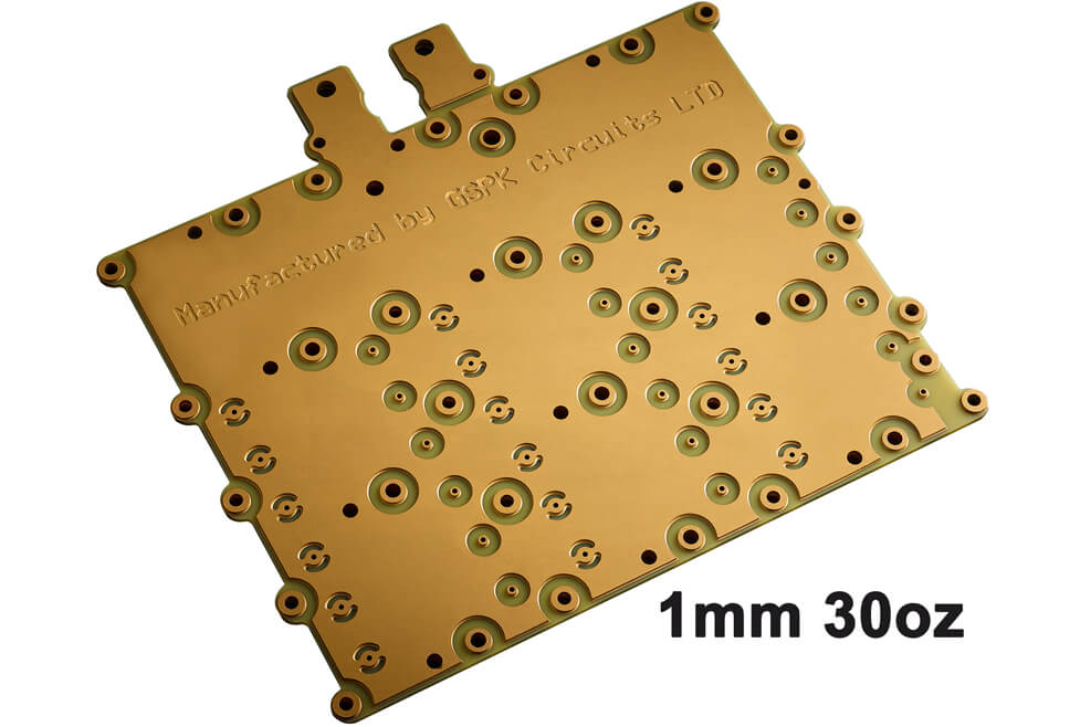
These PCBs are becoming increasingly necessary as more industrial applications call for more robust circuitry for high power. At GSPK we manufacture Extreme Heavy Copper PCBs that will take over 1500 Amps.
Heavy Copper and Extreme Heavy Copper PCBs offer benefits such as:
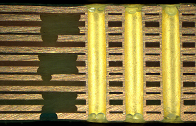
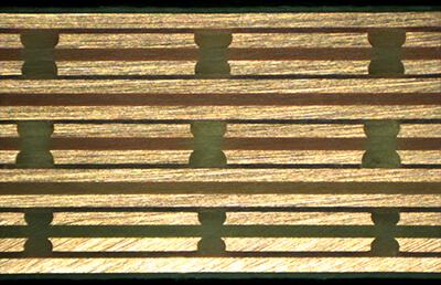
A new development at GSPK with Heavy Copper PCBs is we can embedded part of a copper layer within the PCB core. This copper layer is often referred to as an "inner layer" or a "power plane," and it is used to provide power and ground connections for the components on the board.
Part of the copper tracks are hidden within the board, much like the majority of an iceberg is hidden beneath the surface of the water.
Embedded copper PCBs are used in a variety of electronic devices, particularly those that require high-speed or high-frequency signal processing. By providing a dedicated inner layer for power and ground connections, these PCBs can reduce electromagnetic interference (EMI) and improve signal integrity. They can also help reduce the overall size and weight of a device, since fewer external components are needed to provide power and ground connections.
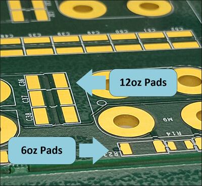
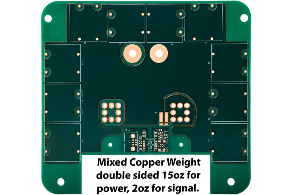
Embedded copper with different copper weights enables greater packaging opportunities and the ability to have the outer layers on one planar level which greatly aids assembly of components.
| Type | Thickness (mm) | Copper Weight (oz) |
|---|---|---|
| Standard Copper | 0.018 - 0.14 | ½ - 4 |
| Heavy Copper | 0.175 - 0.525 | 5 - 15 |
| Extreme Heavy Copper | 0.525 - 2.45 | 15 - 70 |
| Mixed Copper Weights | 1 ½ oz and 30 oz on the same layer (Double Sided) |
| Applications For Heavy Copper | |
|---|---|
| Bus bars - Lower Copper Weight - Lower Cost | Solar Panel Manufactures |
| Power Controllers | High Power Distribution |
| Inverters | Motor Stators |
| Amplification Systems | Planar Transformers |
| Panel Considerations For Heavy Copper | Minimum production is 1 panel | |
|---|---|---|
| Gross | Net (usable) | |
| Manufacturing Panel Size | 457mm x 610mm | 417mm x 570mm |
| Each circuit to have 3mm border for routing | ||
GSPK Circuits Ltd
Wetherby Road, Boroughbridge
North Yorkshire
YO51 9UY
United Kingdom
+44 (0)1423 798 740
enquiries@gspkcircuits.ltd.uk


GSPK Circuits Ltd. is a market leading UK PCB manufacturer & global supplier of Printed Circuit Boards. We focus on Fast-turn PCBs, Prototyping and Specialist PCBs. Our team manages your PCBs and ensures you get a product with the highest quality. Having the 'Lean Champion' status, you're ensured a fast and agile approach to PCB manufacture in one of our world class manufacturing divisions.