
A redesign incorporating a Copper Coin rather than thermal vias proved a great success
A valued customer recently contacted us to see if we could help solve a thermal issue on a PCB.
The Engineering Team at GSPK looked at the design and a Copper Coin was thought to be the ideal solution to improve the thermal performance.
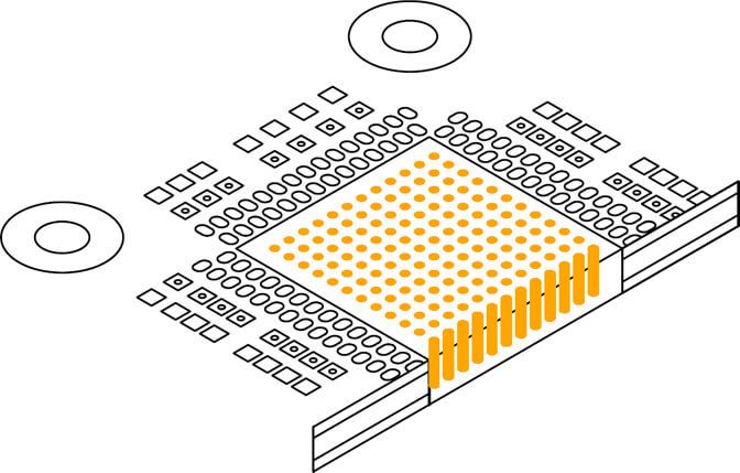
One of the greatest materials for controlling heat while maintaining electrical and/or thermal conductivity is copper with a thermal conductivity of upwards of 400 W/mK but even though the design featured 144 copper filled vias they were not efficient enough, hence the consideration of a copper coin.
A copper coin is a solid piece of copper that is put onto or into the PCB, usually beneath the component or components that require cooling. When compared to a collection of thermal vias copper coins will produce roughly twice the cooling.
Additionally, the copper coin can offer direct contact between the heat-generating component pad and the heat sink in place of thermally conductive material. Compared to other conductive dielectric prepregs, copper has thermal conductivity that is typically 50–200 times better.
 Solid Copper Coin
Regardless of the number of layers in the PCB, copper coins offer the best localised heat transfer solution. The optimal conditions for using this technology are when a single or a small group of PCB components generate most of the heat.
When manufacturing a Copper Coin printed Circuit Board at GSPK Circuits we normally use a solid piece of electrical grade C103 copper bonded directly into the PCB.
The Copper Coin can be bonded through the entire board, leaving it exposed on each side or bonded into the panel from one side only. The Copper Coin is used to dissipate high levels of heat generated by components mounted directly above or below the coin. Grade C103 copper is used due to its high level of electrical conductivity and low susceptivity to hydrogen embrittlement.
Copper Coin technology can be used in combination with other technologies offered by GSPK to provide a solution to the most challenging board designs.
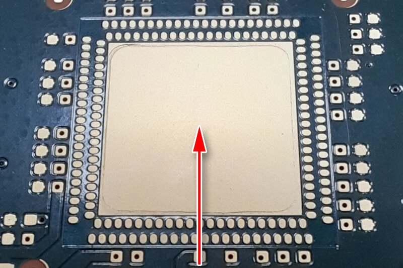
Original Board design
The 4-layer FR4 PCB is to be used in a medical application, where there is a requirement to rapidly apply heat to a BGA analysis device. This is achieved by contacting and heating the underside copper pad, then transferring the energy through the board. The current design was experiencing a thermal transfer issue; as with any FR4, the dielectric had poor thermal conductivity and the series of thermal vias in the board were not proving to be effective in transferring sufficient heat in time.
Recommendations made
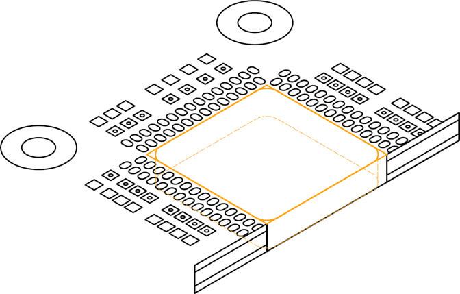
A redesign of the cross section of the PCB was recommended to replace the thermal via holes with a solid copper coin. This would at least double the heat transfer characteristics compared to that achieved with thermal vias.
Redesign Board
144 off 0.2mm vias were replaced with a 9.3 x 9.3mm Copper Coin.
Cross sectional area of copper was increased from 10.2mm3 increased to 86.49mm3, an 8-fold increase in thermal conductivity.
The copper coin was directly bonded into the PCB and electroplated to make the required electrical connections. The remainder of the board remained unchanged, Copper filled blind vias and standard plated through holes utilised in combination with Copper Coin technology for the best overall solution to overcome a serious issue.
The resulting redesign was a great success and is now transferring sufficient heat in the required time.
Date : 23-12-2022
GSPK Circuits Ltd
Wetherby Road, Boroughbridge
North Yorkshire
YO51 9UY
United Kingdom
+44 (0)1423 798 740
enquiries@gspkcircuits.ltd.uk


GSPK Circuits Ltd. is a market leading UK PCB manufacturer & global supplier of Printed Circuit Boards. We focus on Fast-turn PCBs, Prototyping and Specialist PCBs. Our team manages your PCBs and ensures you get a product with the highest quality. Having the 'Lean Champion' status, you're ensured a fast and agile approach to PCB manufacture in one of our world class manufacturing divisions.